
OV-C2-DD-THERMAL · v1.4 · 2026-09-10Download PDF
| Doctype | Design Document |
|---|---|
| Doc id | OV-C2-DD-THERMAL |
| Product line | openvvvf |
| Applies to | chassis-size-2 |
| Version | 1.4 |
| Date | 2026-09-10 |
| Description | IGBT and diode loss analysis, inverter efficiency, and heatsink/baseplate sizing for the Chassis Size 2 traction inverter. |
| Nav order | 241 |
| Normative refs | OV-C2-DD-INDEX, OV-C2-DD-DCLINK-THERMAL, OV-C2-DD-DCLINK-RIPPLE |
System Thermal Analysis
This document estimates the total heat dissipated into the heatsink by the 3-phase traction inverter power stage (3× Mitsubishi CM600DY-24T half-bridge IGBT modules plus the DC-link capacitor bank) and derives the heatsink thermal resistance required for continuous operation. It is the sizing input for the custom heatsink design.
Value marking convention used throughout:
- [DS] - value taken directly from the CM600DY-24T datasheet (Mitsubishi Electric, publication date December 2020); page/figure cited.
- [EST] - engineering estimate derived from datasheet curves (digitized) or standard scaling laws; not explicitly guaranteed by the datasheet.
- [ASM] - modeling assumption about the operating point.
Nomenclature
| Symbol | Meaning | Units |
|---|---|---|
| $A$ | Cross-sectional area (generic) | m² |
| $\cos \varphi$ | Load power factor | - |
| $d(\theta)$ | High-side switch duty cycle as a function of electrical angle | - |
| $E_{on}$ | IGBT turn-on switching energy per pulse | J |
| $E_{off}$ | IGBT turn-off switching energy per pulse | J |
| $E_{rr}$ | Free-wheeling diode reverse-recovery energy per pulse | J |
| $f_{sw}$ | PWM switching frequency | Hz |
| $i(\theta)$ | Instantaneous phase current as a function of electrical angle | A |
| $\hat{I}$ | Peak sinusoidal phase current ($\sqrt{2} \cdot I_{rms}$) | A |
| $I_C$ | IGBT collector DC current | A |
| $I_{CRM}$ | IGBT repetitive peak collector current | A |
| $I_E$ | Free-wheeling diode forward current | A |
| $I_{rms}$ | RMS phase current | A |
| $k$ | Thermal conductivity | W/(m·K) |
| $L$ | Length (thermal conduction path) | m |
| $m$ | Modulation index ($V_{ph,pk} / (V_{DC}/2)$) | - |
| $P_{cap}$ | DC-link capacitor bank heat load | W |
| $P_D$ | Free-wheeling diode conduction loss (per diode) | W |
| $P_{heat}$ | Total heat rejected to the heatsink | W |
| $P_{mod}$ | Heat dissipated per IGBT module | W |
| $P_{out}$ | Inverter output power | W |
| $P_Q$ | IGBT conduction loss (per IGBT) | W |
| $P_{semi}$ | Total semiconductor (IGBT + FWD) loss | W |
| $P_{sw,D}$ | Free-wheeling diode switching loss (per diode) | W |
| $P_{sw,Q}$ | IGBT switching loss (per IGBT) | W |
| $Q$ | Heat flow / power | W |
| $Q_G$ | IGBT gate charge | C |
| $Q_{rr}$ | Free-wheeling diode reverse-recovery charge | C |
| $r_{CE}$ | IGBT on-state resistance (chip + lead) | Ω |
| $r_D$ | Free-wheeling diode on-state resistance (chip + lead) | Ω |
| $R_G$ | External gate resistance | Ω |
| $R_{CC'+EE'}$ | Module internal lead resistance | Ω |
| $R_{th}$ | Thermal resistance | K/W |
| $R_{th(c-s)}$ | Module case-to-sink (baseplate-to-heatsink) thermal resistance | K/W |
| $R_{th(j-c)D}$ | Free-wheeling diode junction-to-case thermal resistance | K/W |
| $R_{th(j-c)Q}$ | IGBT junction-to-case thermal resistance | K/W |
| $R_{th(s-a)}$ | Heatsink surface-to-ambient thermal resistance | K/W |
| $t_{dt}$ | PWM dead time | s |
| $t_{rr}$ | Free-wheeling diode reverse-recovery time | s |
| $T_j$ | Semiconductor junction temperature | °C |
| $T_{j,D}$ | Free-wheeling diode junction temperature | °C |
| $T_{j,Q}$ | IGBT junction temperature | °C |
| $T_{jmax}$ / $T_{jop}$ | Maximum / continuous operating junction temperature | °C |
| $T_s$ | Heatsink surface temperature under the module | °C |
| $T_{amb}$ | Ambient temperature | °C |
| $T_C$ | Module case temperature (datasheet reference); equals the module baseplate temperature | °C |
| $T_{vj}$ | Virtual junction temperature | °C |
| $V_{CC}$ | DC-link voltage during switching-test conditions | V |
| $V_{CE(sat)}$ | IGBT collector-emitter saturation voltage | V |
| $V_{CES}$ | IGBT collector-emitter breakdown voltage | V |
| $V_{DC}$ | DC-link voltage | V |
| $V_{EC}$ | Free-wheeling diode forward voltage | V |
| $V_{EC0}$ | Free-wheeling diode threshold voltage (model fit) | V |
| $V_{CE0}$ | IGBT threshold voltage (model fit) | V |
| $V_{GE}$ | Gate-emitter drive voltage | V |
| $V_{ph,pk}$ | Peak phase voltage | V |
| $V_{ph,rms}$ | RMS phase voltage | V |
| $\Delta T$ | Temperature rise / difference | K or °C |
| $\eta$ | Inverter efficiency | - |
| $\lambda$ | Thermal conductivity (e.g., grease) | W/(m·K) |
| $\varphi$ | Current phase lag behind voltage (power-factor angle) | rad |
| $\theta$ | Electrical angle | rad |
References and system inputs
- CM600DY-24T datasheet, Mitsubishi Electric, December 2020 (600 A / 1200 V dual (half-bridge) IGBT module, 62 mm package).
OV-C2-DD-DCLINK-THERMAL- DC-link capacitor bank heat load of ≈40 W at rated ripple, rejected to the heatsink through the standoff/spreader-plate path.- Project README - power stage: 3× CM600DY-24T half-bridge modules (one per phase), SVPWM, DC link 102–320 V (140 V nominal), 600 A class output. Gate drive +15 V / −9 V via onsemi NCV57100 (7 A peak gate current class).
- Hardware designer input (2026-08, v1.1/v1.2): populated external gate resistance $R_G = 2.7 \ \Omega$ (not the 1.0 Ω datasheet test condition); PWM is clamped at 6 kHz maximum (v1.2). 2 kHz is not the operating intent, 16 kHz will not be used, and the 8 kHz point is dropped: it sits next to the ~7.8 kHz series resonance of the electrolytic can branch (
OV-C2-DD-DCLINK-RIPPLE) and is unattractive anyway; 8 kHz rows are kept in the tables for reference only, outside the clamped envelope. - Current convention (v1.3 correction): the "600 A" design figure is peak phase current, not RMS. The design point is 600 A peak = 424 A RMS ($\hat{I} = 600$ A). All design-point loss/temperature tables in this revision are evaluated at 424 A RMS; current-sweep tables are labeled in RMS with the peak equivalent noted where relevant.
OV-C2-DD-DCLINK-RIPPLE- DC-link ripple derivation: bank ripple is 0.511 A RMS per amp of phase current (RMS); the 60-can electrolytic bank is ripple-limited above ~330 A RMS (~465 A peak) continuous. Basis for the continuous/peak rating in §6.4.
Datasheet parameters used (CM600DY-24T)
Ratings and electrical characteristics
| Parameter | Value | Conditions | Source | Mark |
|---|---|---|---|---|
| $V_{CES}$ | 1200 V | G–E shorted | Datasheet p.2, Maximum Ratings | [DS] |
| $I_C$ (DC) | 600 A | $T_C = 144 \ ^\circ\text{C}$ | Datasheet p.2 | [DS] |
| $I_{CRM}$ | 1200 A | repetitive pulse | Datasheet p.2 | [DS] |
| $V_{CE(sat)}$, chip | 1.55 V typ / 1.80 V max | $I_C = 600$ A, $V_{GE} = 15$ V, $T_{vj} = 25 \ ^\circ\text{C}$ | Datasheet p.2, Electrical Characteristics | [DS] |
| $V_{CE(sat)}$, chip | 1.75 V typ | $I_C = 600$ A, $V_{GE} = 15$ V, $T_{vj} = 125 \ ^\circ\text{C}$ | Datasheet p.2 | [DS] |
| $V_{CE(sat)}$, chip | 1.80 V typ | $I_C = 600$ A, $V_{GE} = 15$ V, $T_{vj} = 150 \ ^\circ\text{C}$ | Datasheet p.2 | [DS] |
| $V_{CE(sat)}$, terminal | 1.75 / 2.00 / 2.10 V typ (2.05 V max at 25 °C) | $I_C = 600$ A, 25 / 125 / 150 °C | Datasheet p.2 | [DS] |
| $V_{EC}$, chip (FWD) | 1.65 V typ (2.00 V max at 25 °C) | $I_E = 600$ A, 25 / 125 / 150 °C | Datasheet p.2 | [DS] |
| $V_{EC}$, terminal (FWD) | 1.85 / 2.00 / 2.00 V typ | $I_E = 600$ A, 25 / 125 / 150 °C | Datasheet p.2 | [DS] |
| $E_{on}$ | 56.6 mJ typ | $V_{CC} = 600$ V, $I_C = 600$ A, $V_{GE} = \pm 15$ V, $R_G = 1.0 \ \Omega$, $T_{vj} = 150 \ ^\circ\text{C}$, inductive load | Datasheet p.2 | [DS] |
| $E_{off}$ | 64.3 mJ typ | same conditions | Datasheet p.2 | [DS] |
| $E_{rr}$ | 38.2 mJ typ | same conditions, $I_E = 600$ A | Datasheet p.2 | [DS] |
| $Q_{rr}$ / $t_{rr}$ | 60 µC typ / 400 ns max | $V_{CC} = 600$ V, $I_E = 600$ A, $R_G = 1.0 \ \Omega$ | Datasheet p.2 | [DS] |
| $Q_G$ | 3.7 µC typ | $V_{CC} = 600$ V, $I_C = 600$ A, $V_{GE} = 15$ V | Datasheet p.2 | [DS] |
| $R_{CC'+EE'}$ (internal lead R) | 0.3 mΩ typ | per switch, $T_C = 25 \ ^\circ\text{C}$ | Datasheet p.2 | [DS] |
| Switching times | $t_{d(on)} \le 500$ ns, $t_r \le 200$ ns, $t_{d(off)} \le 600$ ns, $t_f \le 300$ ns | $V_{CC} = 600$ V, $I_C = 600$ A, $R_G = 1.0 \ \Omega$ | Datasheet p.2 | [DS] |
| $T_{jop}$ / $T_{jmax}$ | $-40 \dots +150 \ ^\circ\text{C}$ continuous / $175 \ ^\circ\text{C}$ instantaneous | - | Datasheet p.2 | [DS] |
| Recommended operating point | $V_{CC} = 600$ V typ (850 V max), $V_{GE(on)} = 15$ V, $R_G = 1.0$–$10 \ \Omega$ | - | Datasheet p.4 | [DS] |
| Populated gate drive | $R_G = 2.7 \ \Omega$ external, $V_{GE} = +15 \ \text{V} / -9 \ \text{V}$, NCV57100 7 A driver | - | Hardware designer input, 2026-08 | [ASM] |
Thermal resistances
| Parameter | Value | Per | Source | Mark |
|---|---|---|---|---|
| $R_{th(j-c)Q}$ | 24 K/kW max (= 0.024 K/W) | one inverter IGBT | Datasheet p.3, Thermal Resistance | [DS] |
| $R_{th(j-c)D}$ | 42 K/kW max (= 0.042 K/W) | one inverter FWD | Datasheet p.3 | [DS] |
| $R_{th(c-s)}$ | 13.3 K/kW typ (= 0.0133 K/W) | one module (grease $\lambda = 3.0$ W/(m·K), 50 µm) | Datasheet p.3, note 6 | [DS] |
Note: $R_{th(c-s)}$ is a typical value; no maximum is given. Grease ageing/pump-out (datasheet note 8) can raise it over life - covered by the heatsink margin policy in §6.
Device model parameters digitized from datasheet curves
Conduction models use the standard $V_0 + r \cdot I$ straight-line fit to the datasheet output/saturation curves at $T_{vj} = 125 \ ^\circ\text{C}$ (chip values), with the internal lead resistance $R_{CC'+EE'} = 0.3 \ \text{m}\Omega$ added because it dissipates heat inside the module:
| Model parameter | Value | Basis | Mark |
|---|---|---|---|
| $V_{CE0}$ | 1.15 V | Fit to $V_{CE(sat)}$ vs $I_C$ curve, chip, 125 °C (datasheet p.6, "Collector-Emitter Saturation Voltage Characteristics"); fit passes through (300 A, 1.45 V), (600 A, 1.75 V), (900 A, 2.05 V) | [EST] |
| $r_{CE}$ | 1.0 mΩ (+ 0.3 mΩ lead = 1.3 mΩ used) | same figure + p.2 lead resistance | [EST] |
| $V_{EC0}$ | 1.15 V | Fit to FWD forward curve, chip, 125 °C (datasheet p.6, "Free Wheeling Diode Forward Characteristics"); through (300 A, 1.38 V), (600 A, 1.65 V), (1200 A, 2.10 V) | [EST] |
| $r_D$ | 0.8 mΩ (+ 0.3 mΩ lead = 1.1 mΩ used) | same figure + p.2 lead resistance | [EST] |
Switching energy models (datasheet p.7, "Half-Bridge Switching Characteristics - switching energy vs collector/emitter current", $V_{CC} = 600$ V, $V_{GE} = \pm 15$ V, $R_G = 1.0 \ \Omega$; the solid $T_{vj} = 150 \ ^\circ\text{C}$ curves were used, anchored exactly at the p.2 table values at 600 A; the dashed 125 °C curves lie ≈5–10 % lower, so the 150 °C curves are conservative at the 125 °C operating point):
| $I_C$ / $I_E$ | $E_{on}$ | $E_{off}$ | $E_{rr}$ | Mark |
|---|---|---|---|---|
| 300 A | ≈ 30 mJ (fit 28 mJ) | ≈ 37 mJ | ≈ 31 mJ | [EST] |
| 600 A | 56.6 mJ | 64.3 mJ | 38.2 mJ | [DS] anchor |
| 850 A | ≈ 106 mJ | ≈ 94 mJ | ≈ 39 mJ | [EST] |
| 1200 A | ≈ 180 mJ | ≈ 130 mJ | ≈ 39 mJ | [EST] |
Piecewise-linear interpolation of these anchor points is used in the model. Digitization uncertainty is about ±5 % (line thickness / anti-aliasing). Note $E_{on}$ is markedly superlinear above 600 A, and $E_{rr}$ saturates above ≈700 A.
Scaling laws applied (not given in the datasheet):
- Voltage scaling: $E(V_{DC}) = E_{600\text{V}} \cdot (V_{DC} / 600 \ \text{V})$. Standard first-order scaling of switching energy with bus voltage. [EST]
- Temperature: 150 °C energy curves used at the 125 °C operating point (conservative). Conduction parameters at 125 °C. [EST]
- Gate conditions: datasheet energies are at $V_{GE} = \pm 15$ V and $R_G = 1.0 \ \Omega$; the inverter drives +15 V / −9 V with a populated $R_G = 2.7 \ \Omega$. The $V_{GE(off)} = -9$ V vs −15 V difference is assumed negligible for the energies. The $R_G$ increase is corrected as follows: the datasheet p.7 $E$ vs $R_G$ figure shows $E_{on}$ roughly tripling at $R_G = 10 \ \Omega$; interpolating linearly in $R_G$ between the 1.0 Ω table value and 3× at 10 Ω gives an $E_{on}$ multiplier of $1 + 2 \cdot (2.7 - 1)/9 \approx 1.38$ at 2.7 Ω. $E_{off}$ and $E_{rr}$ are held at their 1.0 Ω values because no $R_G$-dependent curve for them has been digitized into this model; their $R_G$ dependence is typically much weaker than $E_{on}$'s, but this is unverified here. This is a datasheet-curve interpolation, not a measurement. [ASM] - pin all three energies with a double-pulse test at the populated $R_G = 2.7 \ \Omega$ and +15 V / −9 V gate supplies.
Loss model and assumptions
Assumptions [ASM]
- 3 half-bridge modules, one per phase, symmetrical sharing.
- Modulation index $m = 1.0$, defined as $V_{ph,pk} = m \cdot V_{DC}/2$ (within the linear SVPWM range, which extends to $m = 1.15$ in this convention).
- Sinusoidal phase current $i(\theta) = \hat{I} \cdot \sin \theta$ with $\hat{I} = \sqrt{2} \cdot I_{rms}$.
- Load power factor $\cos \varphi = 0.8$ (traction motor at rated point).
- Junction operating point $T_j = 125 \ ^\circ\text{C}$ (continuous rating is 150 °C; 125 °C leaves margin).
- Switching frequency: per designer intent the PWM is clamped at 6 kHz maximum (v1.2); 2 kHz is retained as a reference point only, 8 kHz is outside the clamped envelope (kept in tables for reference), and 16 kHz is out of scope (will not be used).
- Switching energies include the $R_G = 2.7 \ \Omega$ correction of §2.3: $E_{on}$ multiplied by ≈1.38, $E_{off}$ and $E_{rr}$ unchanged. [ASM]
- Dead time (0.5–4 µs configurable): the extra FWD conduction during dead time adds ≈ $V_{EC} \cdot \langle i \rangle \cdot 2 \cdot t_{dt} \cdot f_{sw} \approx 5$ W per leg (~15 W total) at the 600 A peak (424 A RMS) design point / 2 kHz / 2 µs - under 1 % of total heat, neglected.
- Gate-drive power ($Q_G \cdot \Delta V_{GE} \cdot f_{sw} \approx 0.2$ W per switch, ≈1 W total) is dissipated in the gate resistors/driver, not the module - excluded.
- $E_{on}$ as measured in the datasheet half-bridge circuit already contains the turn-on impact of the opposing diode's reverse recovery; $E_{rr}$ is counted once, in the diode (standard datasheet convention).
Formulas
High-side fundamental duty cycle of one leg (identical for SPWM and SVPWM to first order; third-harmonic injection does not change the fundamental average that sets the IGBT/FWD conduction split):
$$i(\theta) = \hat{I} \cdot \sin \theta \qquad \hat{I} = \sqrt{2} \cdot I_{rms}$$
$$d(\theta) = \frac{1}{2} \cdot \left(1 + m \cdot \sin(\theta - \varphi)\right)$$
Conduction loss per IGBT and per FWD (standard 2-level bridge result, integrating $v(i) \cdot i \cdot d(\theta)$ over the positive current half-wave):
$$P_Q = V_{CE0} \cdot \hat{I} \cdot \left(\frac{1}{2\pi} + \frac{m \cos \varphi}{8}\right) + r_{CE} \cdot \hat{I}^2 \cdot \left(\frac{1}{8} + \frac{m \cos \varphi}{3\pi}\right) \qquad \text{[per IGBT]}$$
$$P_D = V_{EC0} \cdot \hat{I} \cdot \left(\frac{1}{2\pi} - \frac{m \cos \varphi}{8}\right) + r_D \cdot \hat{I}^2 \cdot \left(\frac{1}{8} - \frac{m \cos \varphi}{3\pi}\right) \qquad \text{[per FWD]}$$
Switching loss, averaging the digitized energy curves over the sine half-wave and scaling with bus voltage:
$$P_{sw,Q} = f_{sw} \cdot \frac{V_{DC}}{600 \ \text{V}} \cdot \frac{1}{2\pi} \int_{0}^{\pi} \left[ E_{on}(i(\theta)) + E_{off}(i(\theta)) \right] d\theta \qquad \text{[per IGBT]}$$
$$P_{sw,D} = f_{sw} \cdot \frac{V_{DC}}{600 \ \text{V}} \cdot \frac{1}{2\pi} \int_{0}^{\pi} E_{rr}(i(\theta)) \, d\theta \qquad \text{[per FWD]}$$
Totals for the bridge (6 IGBTs + 6 FWDs) and the heatsink:
$$P_{semi} = 6 \cdot (P_Q + P_D + P_{sw,Q} + P_{sw,D})$$
$$P_{heat} = P_{semi} + P_{cap} \qquad P_{cap} = 40 \ \text{W}$$
$$P_{out} = 3 \cdot V_{ph,rms} \cdot I_{rms} \cdot \cos \varphi = \frac{3 \cdot m \cdot V_{DC} \cdot I_{rms} \cdot \cos \varphi}{2\sqrt{2}}$$
$$\eta = \frac{P_{out}}{P_{out} + P_{heat}}$$
Per-module dissipation (for the thermal chain):
$$P_{mod} = \frac{P_{semi}}{3}$$
Heat vs phase current
Total heat rejected to the heatsink (IGBT + FWD conduction and switching, plus 40 W capacitor heat), $m = 1.0$, $\cos \varphi = 0.8$, $R_G = 2.7 \ \Omega$ ($E_{on} \times 1.38$). Currents are RMS phase current; the design point is 424 A RMS = 600 A peak (bold row). The 600 A RMS row corresponds to 848 A peak, outside the rated envelope, and is retained only as the sweep bound.
| $I_{phase}$ (A rms) | IGBT cond., 6× (W) | FWD cond., 6× (W) | Switching, 6× @140 V / 2 kHz (W) | Caps (W) | Total @140 V / 2 kHz (W) | Total @320 V / 2 kHz (W) | Total @320 V / 6 kHz (W) | Total @320 V / 8 kHz (W) |
|---|---|---|---|---|---|---|---|---|
| 50 | 135 | 30 | 47 | 40 | 252 | 312 | 527 | 635 |
| 100 | 286 | 63 | 65 | 40 | 454 | 537 | 835 | 983 |
| 150 | 453 | 99 | 83 | 40 | 675 | 781 | 1161 | 1351 |
| 200 | 637 | 137 | 101 | 40 | 915 | 1045 | 1507 | 1738 |
| 250 | 837 | 177 | 118 | 40 | 1173 | 1325 | 1867 | 2137 |
| 300 | 1053 | 221 | 135 | 40 | 1449 | 1623 | 2239 | 2548 |
| 350 | 1286 | 267 | 151 | 40 | 1744 | 1938 | 2629 | 2974 |
| 400 | 1535 | 316 | 167 | 40 | 2058 | 2273 | 3036 | 3418 |
| 424 (600 A peak) | 1662 | 342 | 175 | 40 | 2217 | 2442 | 3241 | 3641 |
| 450 | 1801 | 367 | 184 | 40 | 2392 | 2629 | 3470 | 3890 |
| 500 | 2083 | 421 | 204 | 40 | 2748 | 3010 | 3942 | 4408 |
| 550 | 2381 | 478 | 225 | 40 | 3124 | 3414 | 4443 | 4957 |
| 600 (= 848 A pk, sweep bound) | 2696 | 537 | 247 | 40 | 3520 | 3838 | 4967 | 5532 |
Conduction dominates at 2 kHz (switching is only ≈7 % of semiconductor loss at 140 V / 600 A RMS - the 848 A pk envelope-sweep bound row in the table above, not a rating - because the energies scale with $V_{DC}/600 \ \text{V}$). At 320 V / 6 kHz switching is ≈37 % of the 3.2 kW semiconductor loss at the 424 A RMS design point, and at 8 kHz ≈44 % of 3.6 kW. The 40 W capacitor heat is unchanged from v1.0; its derivation and the bank ripple-rating check are in OV-C2-DD-DCLINK-RIPPLE (40 W corresponds to ~240 A RMS operation; the bank loss at 424 A RMS is ~110 - 125 W with the [ASM] ESR ratio there - see that document's comparison section).
Loss breakdown at two reference currents (140 V, 2 kHz, $R_G = 2.7 \ \Omega$):
| Quantity | 300 A rms (424 A pk) | 424 A rms (600 A pk, design point) |
|---|---|---|
| Per-IGBT conduction | 176 W | 277 W |
| Per-FWD conduction | 37 W | 57 W |
| Per-IGBT switching | 16 W | 22 W |
| Per-FWD switching ($E_{rr}$) | 6 W | 7 W |
| Per module ($P_{semi}/3$) | 470 W | 726 W |
| Semiconductor total | 1409 W | 2177 W |
| Total to heatsink (incl. 40 W caps) | 1449 W | 2217 W |
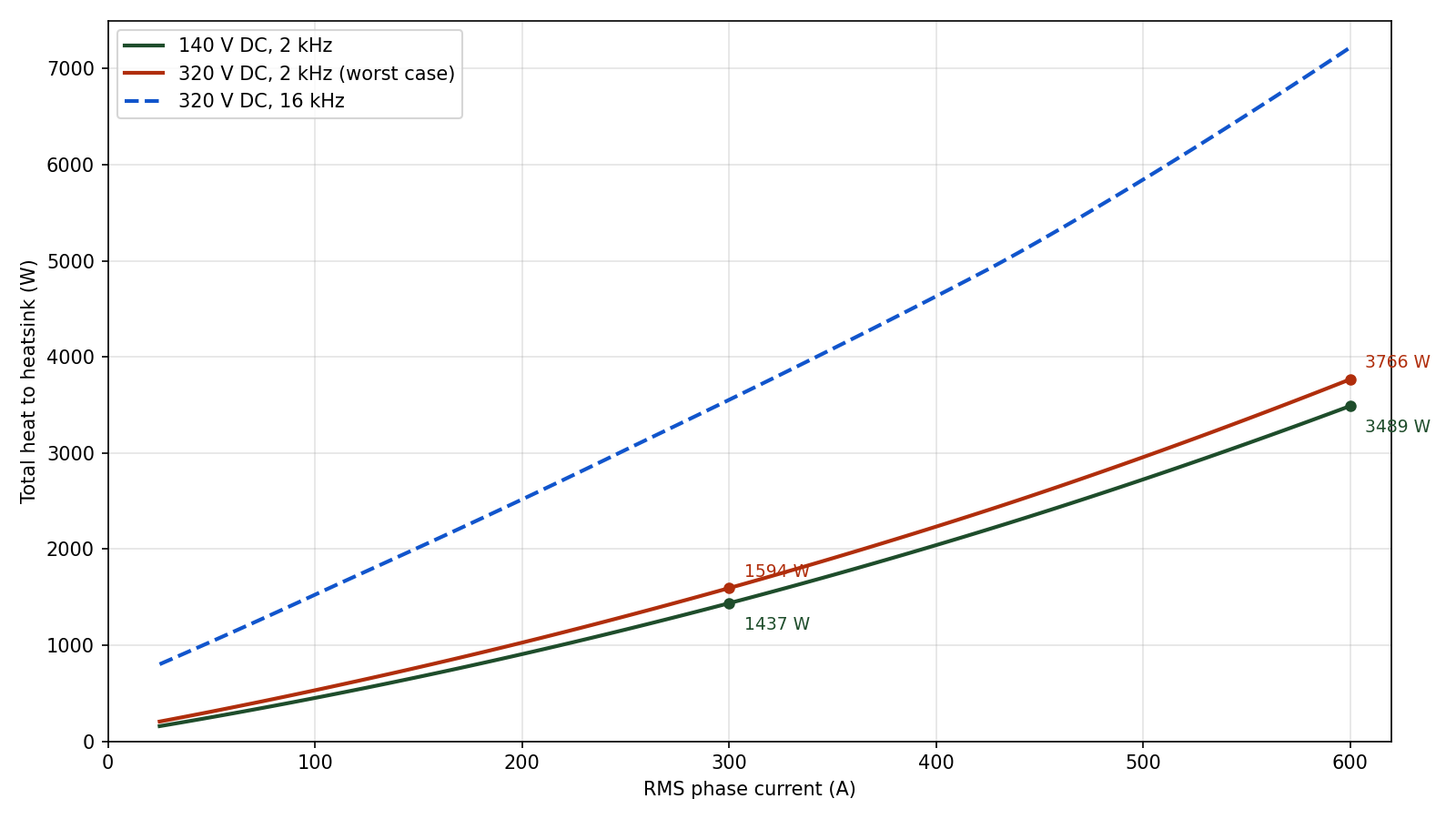
(The plotted curves are from the v1.0 model at $R_G = 1.0 \ \Omega$; regenerating them against the v1.1 numbers is an open item. The table above is authoritative.)
Inverter efficiency vs phase current
$$\eta = \frac{P_{out}}{P_{out} + P_{heat}} \quad \text{at } m = 1.0, \ \cos \varphi = 0.8, \ 2 \ \text{kHz}, \ R_G = 2.7 \ \Omega$$
including the 40 W capacitor heat.
$$P_{out} = \frac{3 \cdot m \cdot V_{DC} \cdot I_{rms} \cdot \cos \varphi}{2\sqrt{2}}$$
i.e., each bus voltage runs at its rated fundamental output voltage ($P_{out}$ at the 424 A RMS / 600 A peak design point: 37 kW @102 V, 50 kW @140 V, 72 kW @200 V, 115 kW @320 V; table currents are RMS).
| $I_{phase}$ (A rms) | $\eta$ @102 V (%) | $\eta$ @140 V (%) | $\eta$ @200 V (%) | $\eta$ @320 V (%) |
|---|---|---|---|---|
| 50 | 94.8 | 95.9 | 96.9 | 97.8 |
| 100 | 95.2 | 96.3 | 97.2 | 98.1 |
| 150 | 95.2 | 96.4 | 97.3 | 98.1 |
| 200 | 95.1 | 96.3 | 97.3 | 98.1 |
| 250 | 95.0 | 96.2 | 97.2 | 98.1 |
| 300 | 94.8 | 96.1 | 97.1 | 98.0 |
| 350 | 94.7 | 96.0 | 97.0 | 98.0 |
| 400 | 94.5 | 95.8 | 97.0 | 98.0 |
| 450 | 94.3 | 95.7 | 96.9 | 97.9 |
| 500 | 94.1 | 95.6 | 96.8 | 97.8 |
| 550 | 94.0 | 95.4 | 96.7 | 97.8 |
| 600 | 93.8 | 95.3 | 96.6 | 97.7 |
At the 140 V nominal bus the efficiency peaks at ≈96.4 % around 150–200 A and falls to 95.3 % at 600 A, because conduction loss grows faster than output power (the $r \cdot I^2$ term). Higher bus voltages are more efficient at the same current because conduction loss is unchanged while output power scales with $V_{DC}$.
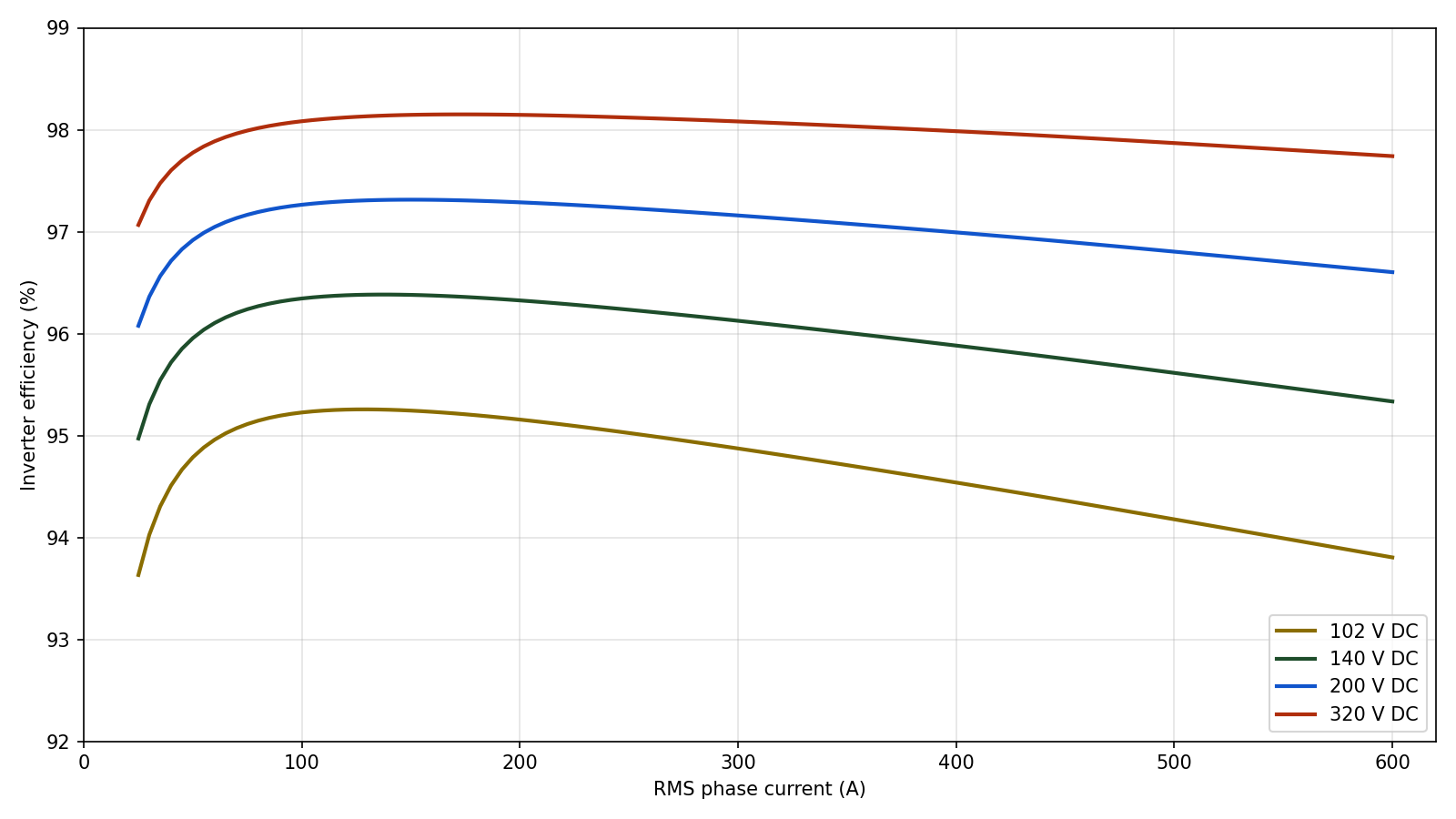
(Plotted curves are v1.0 / $R_G = 1.0 \ \Omega$; see the note in §4. Efficiency at 6–8 kHz is lower than tabulated here, by roughly 0.5–1 percentage point at 320 V / 600 A.)
Heatsink sizing
Thermal chain
Steady-state 1-D chain from junction to ambient for the hottest IGBT of a module:
$$T_s = T_{amb} + P_{heat} \cdot R_{th(s-a)}$$
$$T_C = T_s + P_{mod} \cdot R_{th(c-s)}$$
$$T_{j,Q} = T_C + (P_Q + P_{sw,Q}) \cdot R_{th(j-c)Q}$$
$$T_{j,D} = T_C + (P_D + P_{sw,D}) \cdot R_{th(j-c)D}$$
- $R_{th(c-s)} = 13.3$ K/kW typ per module (thermal grease) [DS p.3]
- $R_{th(j-c)Q} = 24$ K/kW max, $R_{th(j-c)D} = 42$ K/kW max [DS p.3]
- Design limits: module baseplate $T_C \le 85 \ ^\circ\text{C}$ at $T_{amb} = 40 \ ^\circ\text{C}$; junction target $T_j \le 125 \ ^\circ\text{C}$ with margin (continuous rating 150 °C [DS]). The 85 °C baseplate limit is also consistent with the firmware NTC monitor (100 °C hard cap on the module-sited NTC). Note the DC-link spreader plate no longer has margin to this limit at the design point: it reaches the FSR-08 derate/SSO band at full load - see §6.3.
Required heatsink thermal resistance
Worst case is 320 V bus (highest switching loss); 140 V nominal shown for reference. All points at $R_G = 2.7 \ \Omega$. 16 kHz is out of scope per designer intent and is no longer evaluated; 8 kHz is shown for reference only (outside the 6 kHz clamped envelope). The 424 A RMS rows are steady-state evaluations at the 600 A peak current; the 330 A RMS row is the continuous rating point (§6.4).
| Operating point | $P_{heat}$ (W) | $P_{mod}$ (W) | $\Delta T_{(c-s)}$ (K) | Max $T_s$ (°C) | Required $R_{th(s-a)}$ | $T_{j,Q}$ check | $T_{j,D}$ check |
|---|---|---|---|---|---|---|---|
| 330 A rms (465 A pk) / 320 V / 6 kHz (continuous rating) | 2471 | 810 | 10.8 | 74.2 | ≤ 0.0139 K/W | 93 °C ✓ | 89 °C ✓ |
| 424 A rms (600 A pk) / 320 V / 2 kHz (reference) | 2442 | 801 | 10.6 | 74.4 | ≤ 0.0141 K/W | 93 °C ✓ | 88 °C ✓ |
| 424 A rms (600 A pk) / 320 V / 6 kHz (peak duty) | 3241 | 1067 | 14.2 | 70.8 | ≤ 0.0095 K/W | 95 °C ✓ | 89 °C ✓ |
| 424 A rms (600 A pk) / 320 V / 8 kHz (beyond envelope) | 3641 | 1200 | 16.0 | 69.0 | ≤ 0.0080 K/W | 96 °C ✓ | 90 °C ✓ |
| 424 A rms (600 A pk) / 140 V / 2 kHz (reference) | 2217 | 726 | 9.7 | 75.3 | ≤ 0.0159 K/W | 92 °C ✓ | 88 °C ✓ |
| 424 A rms (600 A pk) / 140 V / 6 kHz (reference) | 2567 | 842 | 11.2 | 73.8 | ≤ 0.0132 K/W | 93 °C ✓ | 88 °C ✓ |
DC-link plate temperature and the capacitor environment (FSR-08 integration)
Framing (v1.3, per designer): the spreader-plate temperature is not itself a design constraint - the plate matters only as the thermal environment of the DC-link capacitors. The governed quantity is the can temperature (105 °C category rating; FSR-08 capacitor channel: derate at 90 °C, SSO at 105 °C), which equals the plate environment plus the can's internal $I^2 \cdot ESR$ hot-spot rise, minus the convection/radiation credit that the conduction-only plate model ignores. The plate numbers below are therefore informational upper bounds on the capacitor environment, not pass/fail criteria.
The DC-link spreader plate sits on the same heatsink and rises up to +35.0 K over the local heatsink surface under its 40 W reference load (thermal paste path, rev-B 6.35 mm plate with the corrected 63 mm rods, OV-C2-DD-DCLINK-THERMAL v1.3; conservative upper bound, convection/radiation neglected; the rev-A 3.18 mm plate with 55 mm rods gave +40.1 K). Taking the maximum $T_s$ for each operating point above (heatsink sized exactly to the 85 °C baseplate limit) and adding the 35.0 K standoff rise:
| Operating point | Max $T_s$ (°C) | Plate $T_s + 35.0$ K (°C, upper bound) |
|---|---|---|
| 424 A rms (600 A pk) / 320 V / 2 kHz | 74.4 | 109.4 |
| 424 A rms (600 A pk) / 320 V / 6 kHz | 70.8 | 105.8 |
| 424 A rms (600 A pk) / 320 V / 8 kHz (beyond envelope) | 69.0 | 104.0 |
| 424 A rms (600 A pk) / 140 V / 2 kHz | 75.3 | 110.3 |
| 424 A rms (600 A pk) / 140 V / 6 kHz | 73.8 | 108.8 |
| 330 A rms (465 A pk) / 320 V / 6 kHz (continuous) | 74.2 | 109.2 |
Against a fixed heatsink the numbers are lower: with the 0.006 K/W margin-target heatsink from the Guidance section, 424 A RMS / 320 V gives $T_s \approx 55 / 59$ °C at 2 / 6 kHz, i.e. plate ≈ 90 / 94 °C; at the 330 A RMS continuous point $T_s \approx 55$ °C, plate ≈ 90 °C (6 kHz). The apparent cooling at higher loss in the table is the sizing-method artifact discussed in v1.1/v1.2: more loss demands a stronger heatsink for the same 85 °C baseplate limit. [ASM] - the plate numbers inherit the ±20 % spreading uncertainty of the DC-link model and its missing convection/radiation credit, and the plate-to-can thermal coupling is unmodeled.
Open hardware fact (v1.3): where the DC-link capacitor NTC is actually mounted - on the spreader plate vs on/near a can - determines what the FSR-08 90/105 °C thresholds measure. If the NTC reads the plate, the thresholds effectively proxy can temperature, and two things follow: (a) on this conservative plate model with the rev-B 6.35 mm plate and the corrected 63 mm rods the 90 °C derate onset sits at ≈330 A RMS continuous (320 V / 6 kHz, 0.006 K/W heatsink) - essentially coincident with the 330 A RMS ripple-based continuous rating, so if the NTC reads the plate, the effective continuous limit remains NTC-placement-dependent at the margin (with the rev-A 3.18 mm plate the onset was ≈220 A RMS and clearly decided the limit); (b) the thresholds can be revisited once can-vs-plate correlation is measured on the dyno (thermal test plan T-05/T-06). Confirm the NTC location from the DC-link board design and record it here and in OV-C2-DD-DCLINK-THERMAL.
Heat-load caveat (v1.3): the +35.0 K reference rise is at the 40 W plate load, corresponding to ≈242 A RMS phase current. The bank loss scales with current squared (74 W at 330 A RMS, 122 W at 424 A RMS, per OV-C2-DD-DCLINK-RIPPLE); if 100 % of it conducted into the plate the bounds would be ≈120 / ≈160 °C at the continuous/peak points - physically excluded by can self-convection and field experience. The conducted fraction is the open measurement (T-05); see OV-C2-DD-DCLINK-THERMAL §"Effect of capacitor heat load".
What governs the rating: the capacitor constraints that actually bind are (a) per-can ripple current vs the frequency-corrected datasheet rating (sets the 330 A RMS continuous rating, §6.4) and (b) can hot-spot temperature vs 105 °C (bounded at the 60 s peak by the minutes-class can time constant). The semiconductor chain has margin throughout ($T_{j,Q} \le 96$ °C vs the 125 °C target at every table point). The plate/plate-model temperature is retained as the conservative bound on the capacitor environment and as the correlation target for the dyno NTC calibration - not as a rating constraint.
Continuous and peak current rating (v1.3)
Ratings are stated in peak phase current per the IEC 61800-2 style overload convention: a continuous rating plus a time-limited peak, where peak = 600 A for 60 s (424 A RMS). Throughout this document the analysis currents are RMS, with the peak equivalent noted ($\hat{I} = \sqrt{2}\,I_{rms}$). The designer's reservation about peak differing from continuous is addressed by making the peak verifiable: it carries an explicit time limit and a windowed RMS duty requirement (below), so it is a testable envelope, not a marketing number.
Continuous rating: 465 A (330 A RMS) at 6 kHz PWM, 40 °C ambient, with the 0.006 K/W margin-target heatsink. The constraints at 6 kHz:
| Constraint | Limit at 6 kHz | Source |
|---|---|---|
| Electrolytic bank ripple (per-can vs frequency-corrected UCS rating) | 465 A (330 A RMS) (332 A RMS crossing) | OV-C2-DD-DCLINK-RIPPLE |
| DC-link plate < 90 °C (FSR-08 derate onset), conservative bound with rev-B plate and 63 mm rods | ≈330 A RMS (informational; coincident with the ripple limit at the margin) | this document, §6.3 model |
| Junction temperature ($T_{j,Q}$ at 330 A RMS / 320 V) | 93 °C vs 125 °C target (not binding) | this document, §6.2 |
The rating is set by the capacitor ripple: the electrolytic bank binds at 330 A RMS; the plate and the semiconductors do not. At 330 A RMS / 320 V / 6 kHz the model gives $P_{heat} = 2471$ W, $T_s \approx 55$ °C, plate upper bound ≈ 90 °C (rev-B 6.35 mm plate, 63 mm rods, +35.0 K reference rise - at the derate onset on this conservative bound), $T_{j,Q} \approx 93$ °C (far inside the 125 °C target). The rating is stated at the worst-case bus (320 V).
This is a conservative analytical bound, not a measured rating. The conservatisms, itemized:
- The plate model routes 100 % of capacitor heat through the standoff path and credits no convection/radiation; the real rise is below +35.0 K (
OV-C2-DD-DCLINK-THERMAL,OV-C2-DD-DCLINK-RIPPLE§"Interpretation"). - The ripple/ESR model uses an assumed ESR ratio (0.15 × tan δ ceiling) with no published UCS impedance curve; ±50 % would not be surprising (
OV-C2-DD-DCLINK-RIPPLE[ASM]). - The ripple current formula is a stiff-source upper bound; a real battery/dyno source absorbs part of the ripple.
- Worst-case continuous duty at $m = 1.0$, $\cos \varphi = 0.8$, 40 °C ambient; no credit for part-load, cooler ambients, or cans running below their 105 °C category temperature (the ripple check is performed at the 105 °C rating; Nichicon publishes no temperature coefficient for UCS, so no credit is taken for cooler cans).
- Field experience at 100 - 200 A phase current shows the cans running cool, which is consistent with the model at those currents and suggests the bound has real margin at rated current too.
Measured data supersedes this bound when available; the two pinning measurements are listed in OV-C2-DD-DCLINK-RIPPLE §"Continuous and peak rating" (can-branch ripple measurement and can/plate NTC correlation at load).
Peak rating: 600 A (424 A RMS) for 60 s at ≤ 6 kHz, validated by thermal time constants:
- Junction (fast, seconds class): the IGBT junction reaches essentially its steady-state rise well within 60 s; $T_{j,Q} = 95$ °C and $T_{j,D} = 89$ °C at 424 A RMS / 320 V / 6 kHz vs the 125 °C design target. Not binding.
- Heatsink and plate (slow, minutes class [EST]): on the 0.006 K/W heatsink the steady-state plate bound is ≈ 90 °C at the continuous point and ≈ 94 °C at the peak point (rev-B plate, 63 mm rods) - a delta of only ~4 - 5 K, of which a 60 s excursion captures 10 - 33 % (3 - 10 min plate+heatsink time constant [EST]): end-of-peak plate ≈ 90 - 91 °C, around the 90 °C derate onset on this conservative bound.
- Capacitor cans (slow, minutes class [EST]): at 424 A RMS the per-can ripple is 3.61 A RMS, 1.28x the 6 kHz rating (≈1.6x rated $I^2 \cdot ESR$ loss). This exceeds the continuous ripple rating but is time-limited: the winding hot-spot responds with a minutes-class time constant, so a 60 s peak captures only a fraction of the incremental rise from the continuous point; the per-event hot-spot excursion is single-digit K class [EST]. The accumulated lifetime cost is bounded by the duty requirement below. Pin with the can NTC during dyno (thermal test plan T-05/T-06).
- Duty requirement (makes the peak verifiable): RMS phase current over any rolling 10-minute window shall not exceed the 330 A RMS continuous rating. Worked example: after a full 60 s / 424 A RMS peak, the following 9 minutes must stay at ≲ 318 A RMS; shorter or lower peaks relax this proportionally. Firmware shall enforce the windowed RMS limit. With the rev-B plate the end-of-peak plate bound (≈90 - 91 °C) sits at the FSR-08 90 °C derate onset, so the derate response may graze onset on a compliant peak if the NTC reads the plate; the firmware shall tolerate this bounded excursion rather than SSO. If the NTC is can-mounted, the thresholds apply to the can estimate per §6.3.
Why peak ≠ continuous, honestly: continuous 600 A (424 A RMS) operation exceeds the electrolytic ripple rating (1.28x at 424 A RMS), and fixing that costs hardware this chassis does not have (≈77 cans to hold the 6 kHz rating at 424 A RMS, or higher-ripple cans / a film bank - see OV-C2-DD-DCLINK-RIPPLE). The 60 s peak covers real traction duty (acceleration, gradeability, obstacle starts) where high current is inherently transient, while the continuous rating keeps the capacitors inside their datasheet endurance. If a future revision needs higher continuous current, the levers are in OV-C2-DD-DCLINK-RIPPLE (bank changes) plus the measurement campaign that may raise the analytical bound without any hardware change.
Guidance
- Peak 600 A pk (424 A RMS) / 320 V (60 s): $R_{th(s-a)} \le 0.0095$ K/W (9.5 mK/W) at the 6 kHz clamp for the whole three-module heatsink assembly, 40 °C ambient (8.0 mK/W at the out-of-envelope 8 kHz point; 14.1 mK/W at the 2 kHz reference). With ≥25 % engineering margin (grease ageing, digitization/typ-value uncertainty, module-to-module variation, fouling), the design target is ≈ 0.007 K/W or better; the margin-target value used for the rating analysis in §6.4 is 0.006 K/W, i.e. ≈37 % margin against the 6 kHz peak requirement. All of these are outside natural-convection territory (a very large natural-convection sink is ≈0.1–0.5 K/W); 6 kHz at high current requires a liquid cold plate.
- Continuous 330 A RMS (465 A pk) / 320 V / 6 kHz (rated point): $R_{th(s-a)} \le 0.0139$ K/W for the baseplate constraint; with the 0.006 K/W margin-target heatsink $T_s \approx 55$ °C and the DC-link plate upper bound is ≈ 90 °C, at the 90 °C FSR-08 derate onset on this conservative bound (rev-B plate, 63 mm rods) - see §6.3/§6.4.
- The junction rise is small at the design point ($T_{j,Q} \approx 95 \ ^\circ\text{C}$ at $T_C = 85 \ ^\circ\text{C}$, ≈30 °C margin to the 125 °C target) because $R_{th(j-c)}$ is only 24 K/kW; the baseplate ≤ 85 °C constraint, not the junction, sizes the heatsink. Per-switch dissipation of ≈400 W at 424 A RMS / 320 V / 2 kHz (≈530 W at 6 kHz) is also well inside the module's 6250 W total dissipation rating (datasheet p.2).
- The capacitor bank, not the semiconductors, sets the real full-load limit - the continuous rating is ripple-set (§6.4), and the plate model is the conservative bound on the capacitor environment (§6.3). Any heatsink decision shall be checked against the plate/can temperature, not only the baseplate limit.
- Mounting: thermal grease per datasheet note 6 ($\lambda = 3.0$ W/(m·K), 50 µm), M6 mounting torque 3.5–4.5 N·m (datasheet p.3), baseplate flatness ≤ 200 µm on the centerlines. Verify the three modules are placed so each sees comparable sink temperature.
Sensitivity and notes
- 6 kHz clamp: switching loss scales linearly with $f_{sw}$. At the 600 A RMS (848 A pk, envelope-sweep bound) / 320 V point, total heat rises from 3.8 kW (2 kHz) to 5.0 kW (6 kHz) and 5.5 kW (8 kHz), and the heatsink requirement tightens from 7.3 to 4.7 / 3.7 mK/W (values unchanged; §6.2 sweep-table row). Per designer decision (v1.2) the PWM is clamped at 6 kHz; 8 kHz is dropped (it also sits next to the ~7.8 kHz electrolytic-branch series resonance,
OV-C2-DD-DCLINK-RIPPLE) and 16 kHz is out of scope. 6 kHz at high current means liquid cooling. - Lower power factor: total heat is nearly unchanged (the IGBT $V_0$ term falls while the FWD share rises; at $\cos \varphi = 0.5$, 600 A / 140 V / 2 kHz, $P_{heat} \approx 3.46$ kW vs 3.49 kW at $\cos \varphi = 0.8$), but output power falls proportionally with $\cos \varphi$, so efficiency drops (≈92.8 % at $\cos \varphi = 0.5$, 600 A / 140 V) and heat per kW delivered rises. Regenerative braking ($\cos \varphi < 0$) shifts loss toward the FWDs - $R_{th(j-c)D} = 42$ K/kW keeps the diode junction ≈5 °C cooler than the IGBT at rated point, so this is not binding.
- Typical vs maximum device values: conduction uses typical chip $V_{CE(sat)}/V_{EC}$; the max terminal values are ≈10–15 % higher, and $R_{th(c-s)}$ is a typical (not max) value. The ≥25 % heatsink margin policy covers this.
- 600 A RMS operation: at 600 A RMS the sine peak is 848 A, above the module's 600 A DC rating (at $T_C = 144 \ ^\circ\text{C}$) but within the 1200 A repetitive pulse rating. Per §6.4 (v1.3) the adopted rating is 465 A (330 A RMS) continuous / 600 A (424 A RMS) peak for 60 s: the continuous rating is set by the capacitor ripple (the electrolytic bank binds at 330 A RMS; the plate and the semiconductors do not), and the rated peak operating point is 424 A RMS (600 A pk) for 60 s - the 424 A RMS rows in the tables. The 600 A RMS rows are the 848 A pk envelope-sweep bound, outside the rated envelope, and are retained only as the sweep bound, not as an operating point. Full-load dyno/thermal validation of both ratings is still pending - treat the 600 A RMS rows as the sweep sizing bound, not a validated rating.
- Gate resistance: all switching energies now include the populated $R_G = 2.7 \ \Omega$ correction ($E_{on} \times 1.38$, linear interpolation of the datasheet p.7 $E$ vs $R_G$ curve between 1 Ω and the ≈3× point at 10 Ω; $E_{off}$/$E_{rr}$ unscaled). This is a datasheet-curve interpolation, not a measurement, and the $E_{off}$/$E_{rr}$ $R_G$-dependence is unmodeled [ASM]. Pin $E_{on}$, $E_{off}$, and $E_{rr}$ with a double-pulse test at $R_G = 2.7 \ \Omega$, +15 V / −9 V, representative bus voltage and current; re-run this analysis with the measured energies.
- Low-current extrapolation: below ≈100 A the $E_{rr}/E_{off}$ curve extrapolation carries the constant offsets ($E_{off} \approx 8.7$ mJ, $E_{rr} \approx 12$ mJ); the resulting low-current, high-frequency numbers (e.g., 50 A / 8 kHz) are the least accurate in this document, ±15 %.
- Not modeled: stray-inductance overshoot losses, module NTC self-heating, busbar/terminal ohmic heating into the heatsink (small vs 3.5 kW), and heatsink thermal spreading between modules (left to the heatsink detailed design). Ambient 40 °C is assumed at the heatsink inlet; inside a sealed chassis, derate accordingly.
- Firmware tie-in: the real-time loss estimator uses the same model structure ($V_{ce0}/R_{ce}$ conduction + $E_{on}/E_{off}$ curves + $R_{th}$ chain); the parameters in §2.3 are the recommended calibration set for it.
Revision History
| Version | Date | Changes |
|---|---|---|
| 1.0 | 2026-07-17 | Initial release. |
| 1.1 | 2026-08-20 | Engineering revision from hardware-designer input: populated gate drive is $R_G = 2.7 \ \Omega$, +15 V / −9 V, NCV57100 7 A class (was: datasheet $R_G = 1.0 \ \Omega$ assumption). $E_{on}$ scaled ×1.38 by linear interpolation of the datasheet $E$ vs $R_G$ curve; $E_{off}$/$E_{rr}$ held (unmodeled $R_G$ dependence, [ASM], double-pulse test open). Operating points updated to designer intent: 6 kHz max continuous, 8 kHz upper bound; 2 kHz demoted to reference; 16 kHz removed as out of scope. All loss, efficiency, and heatsink tables recomputed (600 A / 320 V: 3.8 / 5.0 / 5.5 kW and 7.3 / 4.7 / 3.7 mK/W at 2 / 6 / 8 kHz). New §6.3 integrates the DC-link plate temperature (+40.1 K standoff rise from OV-C2-DD-THERMAL) against FSR-08 thresholds: plate exceeds the 90 °C derate at all full-load points and the 105 °C SSO / capacitor rating at several; the plate, not the IGBTs, is now the binding constraint on the 600 A continuous claim. Plots (PNGs) still show the v1.0 curves; regeneration is an open item. |
| 1.2 | 2026-08-20 | Ratings revision. PWM clamped at 6 kHz max per designer decision; 8 kHz dropped (also adjacent to the ~7.8 kHz electrolytic-branch series resonance per OV-C2-DD-DCLINK-RIPPLE) and retained in tables for reference only. New §6.4 states the IEC 61800-2 style rating: 220 A RMS continuous / 600 A RMS peak for 60 s. The continuous rating is the lower of the electrolytic ripple limit (~330 A, OV-C2-DD-DCLINK-RIPPLE) and the DC-link plate 90 °C FSR-08 constraint (220 A at 320 V / 6 kHz on the 0.006 K/W heatsink), and is documented as a conservative analytical bound with itemized assumptions. The 60 s peak is validated by thermal time constants (junction ~101 °C steady, plate/can excursions bounded to ~92 - 97 °C end-of-peak) and carries a verifiable duty requirement (rolling 10-min RMS ≤ 220 A). Guidance, sensitivity notes, and the 600 A operation note aligned. |
| 1.3 | 2026-08-23 | Current-convention correction and re-rating. The "600 A" design figure is peak phase current (600 A pk = 424 A RMS), not RMS; all design-point loss/temperature tables re-evaluated at 424 A RMS, sweep tables labeled RMS with peak equivalents. Plate framing corrected per designer: the spreader plate is the capacitors' thermal environment, not a design constraint - plate numbers are informational upper bounds, the governed quantity is the can temperature (ripple rating + hot-spot). Continuous rating raised from 220 A RMS to 465 A (330 A RMS), set by the electrolytic ripple limit; peak rating restated as 600 A (424 A RMS) for 60 s with rolling 10-min RMS ≤ 330 A RMS (worked example: ≲318 A RMS for 9 min after a full peak). §6.3 plate table updated to the rev-B 6.35 mm spreader plate and the corrected 63 mm rod length (+35.0 K reference rise, was +40.1 K at 3.18 mm / 55 mm); the plate-proxy derate onset sits at ≈330 A RMS, coincident with the ripple-set rating, so NTC placement may still decide the effective continuous limit at the margin. Heatsink requirements relaxed accordingly (peak: ≤9.5 mK/W at 6 kHz; design target ≈7 mK/W; continuous point ≤13.9 mK/W). Open item added: confirm DC-link capacitor NTC mounting location. |
| 1.4 | 2026-09-10 | Consistency fixes, no rating change: (1) the "600 A RMS operation" sensitivity bullet rewritten to the v1.3 §6.4 rating framing - 465 A (330 A RMS) continuous set by the capacitor ripple (electrolytic bank binds; plate and semiconductors do not), 600 A pk = 424 A RMS rated peak for 60 s, and the 600 A RMS rows identified as the 848 A pk envelope-sweep bound; the bullet had retained the superseded v1.2 framing (220 A RMS continuous, set by the DC-link plate). (2) The 140 V / 600 A switching-share figure (≈7 %) and the 6 kHz-clamp loss/heatsink figures (3.8 / 5.0 / 5.5 kW, 7.3 / 4.7 / 3.7 mK/W) are now explicitly labeled as the 600 A RMS (848 A pk) envelope-sweep bound; values unchanged, consistent with the §6.2 sweep table. (3) Nomenclature deduplicated: the separate $T_c$ / $T_C$ entries merged into a single $T_C$ symbol (module case temperature equals the module baseplate temperature); the thermal-chain equations and the design-limit/guidance text updated from $T_c$ to $T_C$. |
This is a design estimate for heatsink sizing, to be validated by test on the assembled inverter.